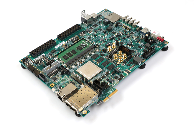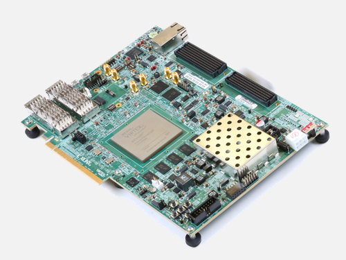
Xilinx Virtex UltraScale+ FPGA VCU118 Evaluation Kit
Product model : EK-U1-VCU118-G
2019-01-10 Times of browsing: 5949-
 Product introduction
 characteristic
 Product specification
 Physical picture
 Resources
The Virtex® UltraScale+™ FPGA VCU118 Evaluation Kit is the ideal development environment for evaluating the cutting edge Virtex UltraScale+ FPGAs. Virtex UltraScale+ devices provide the highest performance and integration capabilities in a FinFET node, including both the highest serial I/O and signal processing bandwidth, as well as the highest on-chip memory density.
This kit is ideal for prototyping applications ranging from 1+ Tb/s networking and data center to fully integrated radar/early-warning systems.
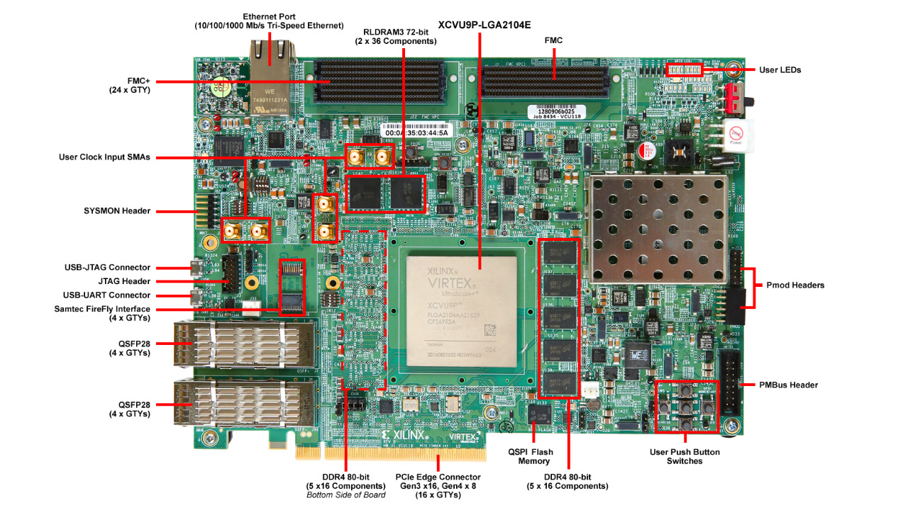
Dual 80-bit DDR4 Component Memory
RLDRAM3 (2x36-bit) Memory
Dual QSFP28 Interfaces
PCIe Gen3 x16 (VCCINT = 0.85V)
VITA 57.4 FMC+ Interface
VITA 57.1 FMC Interface
Samtec FireFly Interface
Configuration
Onboard JTAG configuration circuitry to enable configuration over USB
JTAG header provided for use with Xilinx download cables such as the Platform Cable USB II
QSPI flash memory
Communication & Networking
10/100/1000 Mbps Ethernet (SGMII)
Dual 4x28Gbps QSFP28 cages
Samtec FireFly 4x28Gbps Interface
Dual USB-to-UART Bridge with mico-B USB connector
RJ45 Ethernet connector
PCI Express endpoint Gen3 x 16
Expansion Connectors
FMC+ HSPC connector (24 – 28Gbps GTY Transceivers, 80 differential user defined pairs)
FMC HPC1 connector (58 differential user defined pairs)
PMOD header
IIC
Control & I/O
User Push Buttons (x5)
User DIP Switch (4-position)
PMBUS & System Controller MSP430 for power, clocks, SD-Card and I2C bus switching
Memory
Two 4 GB DDR4 component memory interfaces (five [256 Mb x 16] devices each)
4 MB RLD3 component memory interfaces (five [256 Mb x 16] devices each)IIC EEPROM: 8Kb
Micro Secure Digital (SD) connector 1Gb Quad SPI Flash
Clocking
SI5335A Quad Clock Generator
Si570 IIC Programmable LVDS Clock Generator
SI5328C Clock Multiplier and Jitter Attenuator
2x SMA MGT Reference Clock inputs
1 SMA User Clock input
Display
Users & Status LEDs
Power
12V wall adapter or ATX
